When selecting IGBTs, the designer is faced with a number of architectural choices that can favor one form of IGBT, such as symmetric versus asymmetric blocking, over another. This article will review the design options provided by different IGBT architectures.
The insulated gate bipolar transistor (IGBT) is a common choice for motor-drive applications thanks to its high blocking voltage and low cost compared to power MOSFETs with similar voltage ratings. The technology allows for the design of variable-frequency drives, which are seen as good for energy-efficient systems.
The IGBT provides the switching capability needed to drive the important inverter stage. Typically, a 600 V blocking-voltage rating is needed for drives operating from a 200-240 VAC mains supply, with 1200 V favored for 460 VAC applications.
The IGBT’s structure evolved from the power MOSFET during the 1980s, in response to the need to increase the blocking voltage. This was achieved by adding an extra PN junction to the drain of MOSFET architecture, creating a bipolar transistor structure and an overall NPNP semiconductor. As with most power transistors made today, the construction of the transistor is vertical rather than horizontal, with the collector of the PNP bipolar transistor placed on the backside of the die. A P or P+ tub that contains N-doped wells links the source/emitter and gate regions. Current flows through this tub into a comparatively wide N-doped drift region into the collector. However, because it has the insulated gate of a MOSFET, the device as a whole remains voltage-controlled rather than current-controlled. The gains of the interlocked bipolar transistors need to be carefully controlled to suppress operation as an NPNP thyristor.
Although it generally offers higher voltage isolation than a MOSFET, the architecture of an IGBT means that it cannot switch as quickly, which limits the switching frequency used in inverters, although recent advances in device construction have pushed effective switching frequency towards 100 kHz. Efficiency in IGBTs is improved by a lower on-state voltage drop than MOSFETs. Furthermore, a high current density allows higher power ratings to be reached with a smaller die than an equivalent MOSET, which improves cost-effectiveness.
Early approaches to IGBT design included symmetric structures, also known as reverse-blocking architectures. These have both forward- and reverse-blocking capabilities, suiting them to AC applications such as matrix (AC-to-AC) converters or three-level inverters. Asymmetric structures maintain only forward blocking capability but tend to be used more widely than symmetric structures because they typically offer a lower on-state voltage drop than symmetric IGBTs. The asymmetric structure suits DC applications such as variable speed motor control. However, IGBTs motor control applications tend to involve an inductive load and are often hard switching, requiring that the IGBT be used in parallel with a freewheeling diode to allow reverse current to flow in these topologies. However, such diodes often offer higher performance than the body diode of an equivalent power MOSFET.
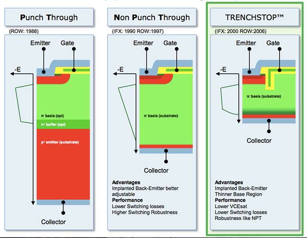
A further distinction in IGBTs is between punch-through (PT) and non-punch-through (NPT) architectures. The PT design is mainly used for lower isolation voltages and uses an N+ region grown on the P+ substrate and collector region. When the device is turned off, the N- drift becomes completely depleted of carriers, an effect that “punches through” into the N+ layer underneath but does not reach completely through it into the collector. The result is a very thin N region that minimizes the turn-on voltage. The additional N+ layer also improves switching speed by reducing the number of excess holes that are injected into the P+ substrate. When the device switches off, these carriers are quickly removed.
Unfortunately, the high doping introduces a large number of minority carriers that need to be removed after IGBT switch off, which increases the switching time and with that, losses in efficiency. This is one major reason for the lower switching frequency compared to power MOSFETs. PT IGBTs can also suffer from thermal runaway.
The NPT was developed to avoid the main problems of the PT architecture and remove the N+ buffer layer. However, they are designed carefully to avoid letting the electric field permeate all the way through to the collector. The transistors are generally made differently to PT devices. Instead of epitaxially forming the N regions on top of a P-doped substrate, NPT transistors are generally made using an N-doped substrate with the collector region grown on the backside.
By thinning wafers to 100 μm or less, it is possible to use a very-lightly-doped collector region and still achieve low resistance and high performance. The use of lighter doping reduces the amount of charge that can be stored in a device when it is conducting, which translates into better switching performance as there are fewer carriers that need to be killed when the device is switched.
The FGP10N60 and FGP15N60 from Fairchild Semiconductor use NPT technology to support a range of motor-drive applications. They offer short-circuit resistance up to 10 μs at 150°C and exhibit a saturation voltage of around 2 V. To support high switching speeds, the transistors exhibit a turn-off delay time of just over 55 ns.
Manufacturers such as International Rectifier moved to a trench structure almost ten years ago. The trench architecture not only allows higher channel density by reducing the effective diameter of the gate and base region, it enhances accumulation-layer charge injection and reduces the effect of the parasitic JFET from which the older planar design suffers. For a given switching frequency, the trench structure reduces both conduction and switching losses compared to conventional PT and NPT structures. Trench IGBTs are now available in a wide range of ratings from a number of vendors. IR’s own range covers the key 600 V and 1200 V blocking voltage ranges.
A typical device, the IRGB4060, is a 1.55 V transistor that is packaged with a soft-recovery reverse diode and offers a turn-off delay time down to 95 ns to support comparatively high switching frequencies.
Adding a field-stop region to a thin-wafer NPT device enables several further improvements in performance. Somewhat similar to the PT concept, the layer stops the electric field, allowing a thinner wafer to be used for the same high breakdown voltage. By controlling the carrier concentration of both the field stop and p+ collector layers it is possible to improve the emitter efficiency of the backside junction. As a result, the field stop provides faster switching on a device with low VCE(sat) made possible by a thinner wafer.
Field-stop technology has made it easier to integrate the freewheeling diode needed in many circuits with the IGBT itself. Examples lie in the TrenchStop family of devices from Infineon Technologies. A number of members of the family form the diode as part of the core IGBT element, allowing reverse current conduction through the device. Others provide diode technologies optimized for applications such as motor control by integrating the diode within the package, such as the IKD06N60RF, which supports switching speeds for motor control up to 30 kHz.

Figure 1: The evolution of IGBTs towards the TrenchStop process at Infineon.
IXYS has developed several series of field-stop architectures, culminating in the Gen3 and Gen4 families. The Gen4 architecture combines the trench topology with the “extreme-light punch-through” (XPT) field-stop design of the Gen3 to support a combination of low on-state voltage and fast turn-off to minimize switching losses.
These devices exhibit a square reverse-bias safe operating area (RBSOA) shape up to the breakdown voltage of 650 V and twice the nominal currents at high temperatures, suiting them to snubberless hard-switching applications. The devices can be co-packaged with anti-parallel diodes and feature high-temperature short-circuit ruggedness of as long as 10 μs at 150°C.
![Image of differences between classic and <a title=]() IXYS XPT architectures" src="http://www.digikey.com.cn/-/media/Images/Article Library/TechZone Articles/2015/February/Process enhancements increase IGBT efficiency for motor drive applications/article-2015february-process-enhancements-increase-fig2.jpg?la=en&ts=04540d29-60fa-4062-b0c5-fb3f1855aa16" title="Differences between classic and IXYS XPT architectures" height="288" width="600"/>
IXYS XPT architectures" src="http://www.digikey.com.cn/-/media/Images/Article Library/TechZone Articles/2015/February/Process enhancements increase IGBT efficiency for motor drive applications/article-2015february-process-enhancements-increase-fig2.jpg?la=en&ts=04540d29-60fa-4062-b0c5-fb3f1855aa16" title="Differences between classic and IXYS XPT architectures" height="288" width="600"/>
Figure 2: Differences between classic and IXYS XPT architectures.
Further advances in device construction such as wafer thinning and improved doping control and device structures will likely increase the performance of IGBTs, providing the power MOSFET with stiff competition in high-efficiency motor-drive applications, particularly where cost is a key consideration.


